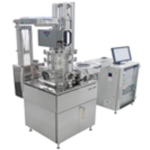
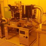
Full flow technology prototyping comprising 100 to 200 steps supported by 30 to 40 tools.
The 8” wafer capability enables the prototypes to easily scale up to the production level.
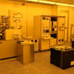
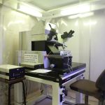
NANO FABRICATION AND PROCESS CAPABILITY
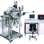
E6NanoFab enables the creation of nanoscale structures and devices with top-down and bottom-up approaches. The facility is equipped to provide maximum flexibility with capabilities to process a variety of materials such as CMOS compatible materials, magnetic materials, III-V & III-N materials, 2D materials and flexible materials.
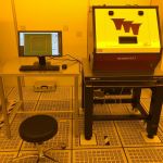
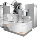
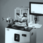
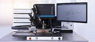
Lithography is a process where a pattern written or transferred to a substrate. It uses light, ions or electron energy into photo and electron sensitive resists. At E6NanoFab, Electron-Beam Lithography, Laser-Writer, and Mask-Aligner tools serve to pattern a variety of materials from sub-10 nanometers up to 100’s of microns over large sample areas.
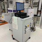
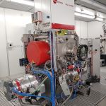
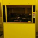
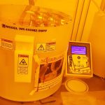
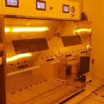
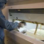
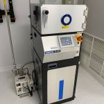
Etching is a process for pattern transfer and surface treatment in micro-nano device fabrication. E6NanoFab makes available dry and wet etching systems to support the diverse process requirement.
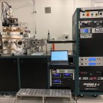
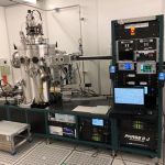
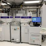
Dry Etching
Multi-chamber cluster tools such as ICP plasma etching and ion beam milling provide strong dry etching capabilities for various materials such as Si, III-V & III-N, oxides, metals, polymers and others.
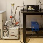
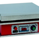
Wet Etching
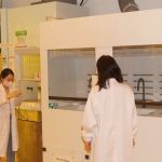
Our dedicated wet-benches support several wet processes such as RCA, standard cleaning, and orientation dependent Si KOH etching.
")